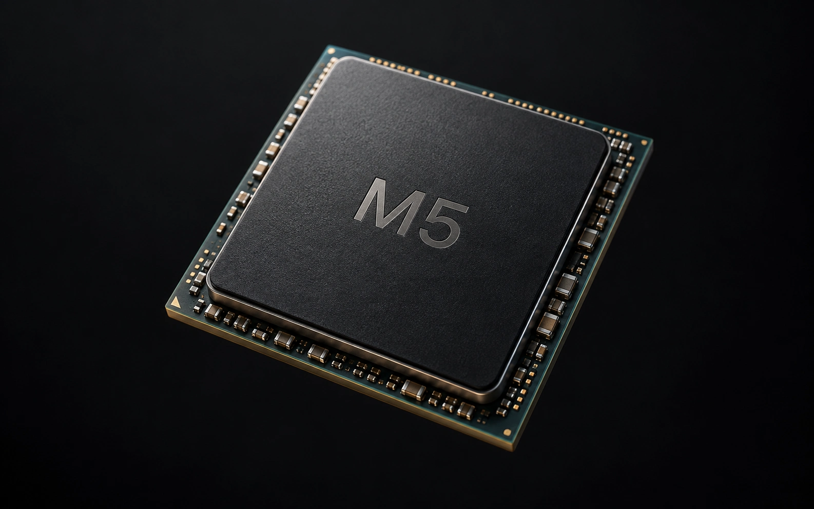
Inside siliconAn M5 exploration

The package

A world
within.

An entire architecture, hidden in a piece of silicon. Let’s go inside.

Scroll to explore

The silicon die

Beneath
the surface.

CPU cores, GPU blocks, and memory share the die. Follow the outlined CPU core as we move into its circuitry.

Silicon · thin-film passivation

The circuit blocks

Order at
every scale.

Inside the core, SRAM arrays sit beside rows of logic cells. Follow their local wiring into the outlined metal stack.

Logic cells · memory arrays

The interconnects

A different
kind of skyline.

Layers of metal carry signals over and between the circuits. Vertical connections, called vias, join one layer to the next.

Copper · dielectric · vias

The transistor

It comes down
to a switch.

A gate controls current through a silicon channel. Repeat this tiny idea billions of times, and a computer emerges.

FinFET · illustrative cutaway
Preparing silicon…

About this exploration

An inward journey.

Inspired by MKBHD and Epic Spaceman’s I shrunk down into an M5 chip.

This is an original, illustrative 3D reconstruction. The internal floorplan, dimensions, colors, and transistor cutaway are explanatory, not a reproduction of Apple’s proprietary chip layout. Scale changes are cinematic.

Apple describes M5 as using third-generation 3-nanometer technology. “3 nm” names a manufacturing generation; it is not the literal size of every transistor feature.

Read Apple’s M5 introduction

Materials are representative: silicon in the fin, doped semiconductor in source/drain regions, conductive metals in the gate and wiring, and an insulating gate dielectric. Hafnium-based high-k dielectrics are a common technology example; this does not identify Apple’s exact gate stack.

The atomic view uses a diamond-cubic silicon model. Spheres mark atoms and rods mark bonds; they are not literal surfaces. A NIST silicon reference gives a lattice constant near 0.543 nm. The nearest-neighbour spacing is a√3/4 ≈ 0.235 nm. These are bulk silicon reference values, not measurements of this illustrated chip.

Electrons are described by probability clouds, not fixed orbits or a bead with a measurable drawn diameter.

Scroll or use the layer navigation to move inward. Reduced-motion settings are respected. View the Blender sequence and render progress.